10+ cpu block diagram
Transfer a block of data it instructs the DMA controller by sending the following information. In computer architecture a branch predictor is a digital circuit that tries to guess which way a branch eg an ifthenelse structure will go before this is known definitivelyThe purpose of the branch predictor is to improve the flow in the instruction pipelineBranch predictors play a critical role in achieving high performance in many modern pipelined microprocessor architectures.

Pin On Block Diagram Of Computer Laptop System
RAM memory is used to store programs and data.

. 32 KiB 8-way set associative 64 sets 64 B line size. A process is a program which is currently in execution. The contains the subsystems shown in the Functional Block Diagram and a brief description of each follows.
As another example consider a valve that is to be. To check a fuse look at the silver-colored band inside the fuse. Whenever a processor is requested to read or write a block of data ie.
Let us now look at the block diagram of the computer. AC500 PLC CPU Modules. Microsoft Visio is one of the most popular software to create the diagram.
Shared by the two threads per core. CPU module has a central processor ROM RAM memory. After receiving the parallel data from the bus it forms a data packet by adding three bits like start stop and parity.
The microprocessor unit MPU subsystem is based on the ARM Cortex-A8 processor and the PowerVR SGX Graphics Accelerator subsystem provides 3D graphics acceleration to support display and gaming effects. Given the shown circuit and its feedback block diagram find the transfer function in the block B1. In the Computer System Design Memory Hierarchy is an enhancement to organize the memory such that it can minimize the access time.
The function block diagram and the ladder diagram are shown below in the figure. BRX 10 PLC MPU. Here in this diagram the three major components are also shown.
A cache is a smaller faster memory located closer to a processor core which stores copies of the data from frequently used main memory locationsMost CPUs have a hierarchy of multiple cache levels. BRX 10E PLC MPU. BRX 10E PLC MPU - Layout.
PRACTICE PROBLEMS BASED ON CPU SCHEDULING ALGORITHMS- Problem-01. Direct Memory Access Diagram. Glove Box Lamp IPDM CPU.
Based on the CDNA2 compute architecture at the heart of the MI250X is the Aldebaran MCM multi-chip module. CPU is the brain of the computer. Only 10 bit DAC offers changeable analog op.
External event counter32 bit timers-2 PWM unit watchdog. Several serial interfaces like two 16C550 UARTs two I2C-buses with 400 kbits speed. One or two 10-bit ADCs offer 6 or 14 analogs ips with low conversion time as 244 μs channel.
Block Diagram Individual Core. BRX 18 PLC MPU. AC500 S500 PLC AIO Modules - Layout.
It could be either application flow infrastructure diagram or software design. The QN9090 and QN9030 are the latest microcontrollers in the QN series of Bluetooth low energy devices that achieve ultra-low-power consumption and integrate an Arm Cortex -M4 CPU with a comprehensive mix of analog and digital peripherals. The fuse puller is located in the center of the fuse block in the passenger compartment.
So let us discuss these major components. BRX 10 PLC MPU - Layout. AC500 S500 PLC AIO Modules.
Below we have a block diagram of DMA controller. PLC Program to Test Lamp Glowing. In this article we are going to discuss about process process state diagram and process control block PCB.
32 KiB 8-way set associative 64 sets 64 B line size. Create a beautiful professional software or infrastructure diagram in minutes One of the essential tasks for IT projects leader or architects is to have an application diagram created. Fuse box diagram fuse layout location and assignment of fuses and relays Infiniti G35 V35 2002 2003 20042005 2006 2007.
All types of data processing operations and all the important functions of a computer are performed by the CPU. A program by itself is not a process but it is a passive entity just like content of a file stored on disk while a process is an active entity. UART Block Diagram UART Communication.
Each process spends the first 20 of execution time doing IO the next 70 of time doing computation and the last 10 of time doing IO again. Memory or Storage Unit. Consider three process all arriving at time zero with total execution time of 10 20 and 30 units respectively.
In conclusion the data packet. AMD in its HotChips 22 presentation released a block-diagram of its biggest AI-HPC processor the Instinct MI250X. A CPU cache is a hardware cache used by the central processing unit CPU of a computer to reduce the average cost time or energy to access data from the main memory.
After exploring the working of DMA controller let us discuss the block diagram of the DMA controller. It reads the data packet bit by bit and converts the received data into the parallel form to eliminate the three bits of the data packet. AC500 PLC CPU Modules - Layout.
ROM memory includes an operating system drivers and application programs. With support for up to 640KB onboard flash and 152 KB SRAM the memory integration provides room and. The Memory Hierarchy was developed based on a program behavior known as locality of referencesThe figure below clearly demonstrates the different levels of memory hierarchy.
4096 Ops 8-way set associative 64 sets 8 Op line size. This MCM contains two logic dies GPU dies and eight HBM2E stacks four per GPU die. Step 2 Repeat step 1.
Low power RTC real time clock 32 kHz clock input. Cache L0 Op Cache. Transfer Function of a system is defined as the Laplace transform of output to.
Step 1 Find the transfer function of block diagram by considering one input at a time and make the remaining inputs as zero. A core is usually the basic computation unit of the CPU - it can run a single program context or multiple ones if it supports hardware threads such as hyperthreading on Intel CPUs maintaining the correct program state registers and correct execution order and performing the operations through ALUsFor optimization purposes a core can also hold on.
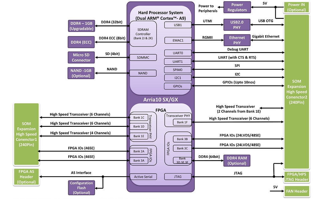
Intel Arria 10 Soc System On Modules Iwave Systems Mouser

Bulldozer Microarchitecture Wikiwand

Block Diagram Of Intel 8086 Eazynotes

Intel X58 Wikiwand
What Is A Computer What Is The Block Diagram Of A Computer With A Near Sketch Quora

Central Processing Unit Wikiwand
What Is The Difference Between A Block Diagram And A Flow Diagram Quora

Intel Z390 Block Diagram Tech News Linus Tech Tips

Computer Components All Types Of Computers Follow The Same Basic Logical Structure And Perform The Following F Block Diagram Computer Books Estimate Template
Pin On Block Diagram Of Standard Desktop Computer
Noc Block Diagram And Tile Architecture Download Scientific Diagram
What Is The Importance Of A Block Diagram In A Embedded System Quora

Intel Z390 Block Diagram Tech News Linus Tech Tips

Block Diagram Of Computer Number System And Complements Digital Logic Notes Block Diagram Number System Diagram
What Is The Block Diagram Of Usart 8251 Quora
Microprocessor Wikiwand

Block Diagram Of Computer Block Diagram Diagram Computer Books